As the world races towards a future dominated by nano-electronics, the demand for smaller, faster, and more efficient devices is driving innovation at an unprecedented pace. In this high-stakes arena, where every nanometer counts, the ability to precisely characterize and optimize the electronic properties of materials at the nanoscale is critical. Scanning Capacitance Microscopy (SCM) has emerged as a powerful tool in this quest, providing unparalleled insights into the electrical properties of semiconductor devices and materials. Let’s explore the strategic importance of SCM in advancing nano-electronics, and how it enables breakthroughs that are reshaping the future of technology.
The Nano-Electronics Revolution: Challenges and Opportunities
Nano-electronics represents the cutting edge of technology, pushing the boundaries of what’s possible in terms of device miniaturization and performance. From quantum dots to ultra-thin transistors, the components at the heart of nano-electronics are incredibly small—often just a few nanometers in size. This extreme miniaturization offers significant advantages, such as faster processing speeds, lower power consumption, and greater device density. However, it also introduces new challenges, particularly in the realm of material characterization and defect analysis.
At these scales, even the slightest variation in material properties can have a profound impact on a device’s performance. Understanding these variations requires tools that can probe the electrical characteristics of materials with nanometer resolution. This is where Scanning Capacitance Microscopy comes into play, offering a unique capability to measure and map the electrical properties of semiconductor materials with extraordinary precision.
What is Scanning Capacitance Microscopy (SCM)?
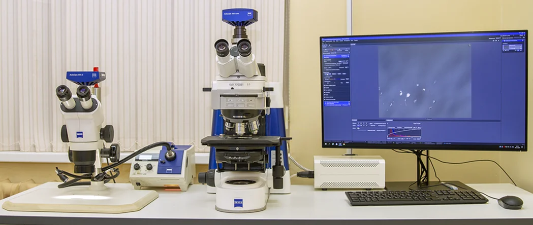
Scanning Capacitance Microscopy (SCM) is a form of scanning probe microscopy that is specifically designed to measure the capacitance between a sharp conducting tip and the surface of a semiconductor material. By applying an alternating voltage to the tip and measuring the resulting capacitance, SCM can provide detailed information about the distribution of charge carriers (electrons and holes) within the material. This allows researchers to map the electrical properties of a sample with nanometer-scale resolution.
The working principle of SCM is based on the concept of capacitance, which is the ability of a system to store an electric charge. In a typical SCM setup, a conductive tip is brought into close proximity to the semiconductor surface, creating a tiny capacitor. As the tip scans across the surface, variations in the local capacitance are measured and recorded, providing a map of the material’s electrical properties.
SCM is particularly valuable for studying semiconductor devices, such as transistors, where the distribution of charge carriers plays a crucial role in determining device performance. By using SCM, researchers can gain insights into the behaviour of these carriers at the nanoscale, helping to identify defects, optimize material properties, and ultimately improve device performance.
Strategic Importance of SCM in Nano-Electronics
The strategic importance of SCM in the field of nano-electronics cannot be overstated. As devices continue to shrink in size, the ability to accurately measure and analyze electrical properties at the nanoscale becomes increasingly critical. SCM provides several key advantages that make it an indispensable tool for researchers and engineers working in this field.
1. High-Resolution Mapping of Electrical Properties
One of the primary advantages of SCM is its ability to provide high-resolution, two-dimensional maps of electrical properties, such as doping concentration and charge distribution. This level of detail is essential for understanding how materials behave at the nanoscale and for identifying any inconsistencies or defects that could impact device performance. Unlike traditional capacitance measurement techniques, which provide average values over large areas, SCM allows for localized measurements, enabling a more detailed and accurate analysis.
2. Non-Destructive Analysis
SCM is a non-destructive technique, meaning that it can be used to analyze delicate or valuable samples without causing any damage. This is particularly important in the field of nano-electronics, where samples are often small and difficult to produce. The non-destructive nature of SCM allows for repeated measurements on the same sample, enabling researchers to track changes over time or after different processing steps.
3. Versatility in Material Analysis
SCM is not limited to any specific type of semiconductor material; it can be applied to a wide range of materials, including silicon, gallium arsenide, and other compound semiconductors. This versatility makes it an invaluable tool for researchers working on the development of new materials for nano-electronic devices. By using SCM, they can explore the electrical properties of these materials in great detail, leading to new insights and innovations.
4. Enhanced Understanding of Device Behavior
In nano-electronics, device behaviour is often influenced by subtle variations in material properties that are difficult to detect with other techniques. SCM’s ability to measure these variations at the nanoscale provides a deeper understanding of how devices operate, helping engineers to design more efficient and reliable components. For example, SCM can be used to study the effects of doping concentration on the performance of transistors, allowing for the optimization of these devices for specific applications.
Real-World Applications of SCM in Nano-Electronics
The practical applications of SCM in the field of nano-electronics are vast and varied. From improving the performance of existing devices to enabling the development of entirely new technologies, SCM plays a crucial role in advancing the state of the art.
One of the most significant applications of SCM is in the development of advanced transistors, such as FinFETs (Fin Field-Effect Transistors) and tunnel FETs. These devices rely on precise control of charge carriers to achieve their high performance, and SCM provides the necessary insights to optimize their design and fabrication. By mapping the distribution of charge carriers within these devices, SCM helps engineers to identify and correct issues that could lead to suboptimal performance or failure.
Another important application of SCM is in the field of quantum computing, where the precise control of electrical properties at the nanoscale is essential for the development of qubits. SCM’s ability to provide detailed information about the distribution of charge carriers makes it an invaluable tool for researchers working on the next generation of quantum devices.
The Role of Leading Laboratories in Advancing SCM Technology
Wintech Nano, a leader in the field of advanced materials analysis, has been at the forefront of developing and refining SCM technology. Their expertise in SCM has enabled them to push the boundaries of what is possible with this powerful technique, providing researchers and engineers with the tools they need to advance the field of nanoelectronics.
Through their innovative approach to SCM, this company has contributed to significant breakthroughs in the understanding of nano-electronic materials and devices. By combining cutting-edge technology with a deep understanding of materials science, this laboratory is helping to drive the next wave of innovation in nano-electronics.
The Future of Nano-Electronics with SCM
As the field of nano-electronics continues to evolve, the importance of precise and accurate material characterization will only grow. SCM’s ability to provide detailed insights into the electrical properties of materials at the nanoscale makes it an essential tool for researchers and engineers working in this cutting-edge field.
Looking to the future, we can expect SCM to play an increasingly important role in the development of new materials and devices, from advanced transistors to quantum computing components. With ongoing advancements in SCM technology, driven by companies, the possibilities for innovation in nano-electronics are virtually limitless.
Conclusion
The advancement of nano-electronics depends on the ability to understand and optimize materials at the smallest scales. Scanning Capacitance Microscopy offers a powerful tool for achieving this goal, providing a high-resolution, non-destructive analysis of electrical properties that is essential for the development of next-generation devices. As researchers and engineers continue to push the boundaries of what’s possible in nano-electronics, SCM will remain at the forefront of innovation, enabling the breakthroughs that will shape the future of technology.